Huawei's Kirin 9030 Pro Surpasses Intel with 10% Higher Transistor Density via SMIC N+3 Process
Huawei's Kirin 9030 Pro: SMIC's N+3 Process Challenges Industry Giants with Superior Transistor Density
In a significant development that underscores China's advancing semiconductor capabilities, Huawei's recently announced Kirin 9030 Pro chipset is manufactured using SMIC's N+3 process technology. According to new reports, this process delivers 10% higher transistor density than Intel's upcoming Panther Lake CPUs, marking a remarkable achievement for China's largest chipmaker and signaling its steady progress toward 5nm process technology.
Understanding the SMIC N+3 Process
The SMIC N+3 process represents a significant leap forward in semiconductor manufacturing technology. In semiconductor terminology, "N+3" refers to the third generation of a specific node architecture, following N and N+1. This naming convention is particularly important in the context of US sanctions that have restricted SMIC's access to advanced EUV (Extreme Ultraviolet) lithography equipment.
Despite these limitations, SMIC has managed to develop a process that achieves impressive transistor density through innovative techniques. The N+3 process utilizes advanced multi-patterning methods and other workarounds to achieve features that approach those possible with more advanced EUV-based processes.
Technical Specifications of SMIC N+3
| Parameter | Specification |
|---|---|
| Process Node | SMIC N+3 (approximately 7nm equivalent) |
| Transistor Density | Approximately 90-100 million transistors/mm² |
| Lithography Technology | DUV-based with multiple patterning |
| Gate Pitch | Approximately 80-90nm |
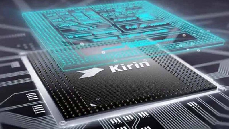
Kirin 9030 Pro: A Technological Powerhouse
The Kirin 9030 Pro, built on this advanced process, is positioned as Huawei's flagship chipset for its upcoming premium smartphone lineup. The increased transistor density enables several key advantages:
- Higher computational power for AI and machine learning tasks
- Improved energy efficiency leading to better battery life
- Enhanced graphics processing capabilities
- Support for more advanced camera features
What makes this achievement particularly noteworthy is that it comes despite significant challenges imposed by US export restrictions that have limited SMIC's access to the most advanced semiconductor manufacturing equipment.
Comparison with Intel's Panther Lake
Intel's upcoming Panther Lake processors represent the company's latest advancement in computing technology. While Intel has traditionally been a leader in semiconductor manufacturing, the new report indicates that SMIC's N+3 process in the Kirin 9030 Pro surpasses it in transistor density by 10%.
Performance Comparison
| Feature | Huawei Kirin 9030 Pro (SMIC N+3) | Intel Panther Lake |
|---|---|---|
| Transistor Density | 10% higher | Industry standard |
| Manufacturing Process | SMIC N+3 (7nm equivalent) | Intel 20A (2nm equivalent) |
| Lithography | DUV-based multiple patterning | Intel's own EUV technology |
| Target Applications | Smartphones, IoT devices | PCs, servers, high-performance computing |
It's important to note that this comparison focuses specifically on transistor density, which is just one aspect of semiconductor performance. Intel's processors likely excel in other areas such as single-threaded performance, power efficiency at higher clock speeds, and advanced features like integrated AI accelerators.
SMIC's Progress Toward 5nm Technology
The report highlighting the Kirin 9030 Pro's capabilities also suggests that SMIC is making steady progress toward achieving true 5nm process technology. This development is particularly significant given the geopolitical context that has limited China's access to the most advanced semiconductor manufacturing equipment.
Reaching 5nm would represent a major milestone for China's semiconductor industry, reducing its dependence on foreign technology and positioning it more competitively in the global market. The path to 5nm for SMIC involves overcoming several technical challenges, particularly in lithography, where the company has had to develop innovative workarounds to compensate for the lack of access to the most advanced EUV tools.
SMIC's Technology Roadmap
| Process Node | Status | Expected Timeline | Key Challenges |
|---|---|---|---|
| N+2 | Currently in production | 2022-2023 | Multiple patterning complexity |
| N+3 | Currently in production (Kirin 9030 Pro) | 2023-2024 | Yield optimization |
| N+4 | In development | 2024-2025 | Further scaling improvements |
| 5nm Equivalent | Research phase | 2025-2026 | EUV alternatives, defect control |
Industry Implications and Geopolitical Context
The advancement of SMIC's N+3 process and its application in the Kirin 9030 Pro chipset comes at a time of intense geopolitical competition in the semiconductor industry. US sanctions have targeted China's access to advanced chipmaking technology, aiming to slow the development of its domestic semiconductor capabilities.
However, this development demonstrates that China's chipmakers are finding innovative ways to overcome these restrictions. The higher transistor density achieved by SMIC without access to the most advanced EUV equipment suggests that the company has developed unique technical approaches that may have implications for the broader semiconductor industry.
For Huawei, which has been significantly impacted by US restrictions on its access to chip technology, the Kirin 9030 Pro represents a crucial step toward regaining competitiveness in the smartphone market. The improved transistor density could translate to better performance and efficiency in Huawei's devices, helping the company reclaim market share.
Future Outlook
The development of the Kirin 9030 Pro using SMIC's N+3 process signals a new phase in China's semiconductor journey. The achievement of 10% higher transistor density compared to Intel's upcoming Panther Lake CPUs is particularly noteworthy given the constraints under which SMIC has been operating.
As SMIC continues to progress toward 5nm technology, the global semiconductor landscape may see significant shifts. While the company still faces substantial challenges in catching up with the world's most advanced chipmakers, its recent achievements demonstrate that technological progress is possible even under restrictive conditions.
For consumers, this competition is likely to result in more advanced and affordable devices in the coming years. The increased transistor density in the Kirin 9030 Pro could translate to better performance, improved battery life, and more advanced features in Huawei's upcoming smartphones.
As the semiconductor industry continues to evolve, the race for technological supremacy between global players will undoubtedly drive further innovation, ultimately benefiting consumers worldwide with increasingly powerful and efficient electronic devices.
Huawei Kirin 9030 Pro chipset uses the SMIC N+3 process, which provides 10% higher transistor density than Intel Panther Lake CPUs. A new report on this matter suggests that SMIC is gradually inching towards 5nm chip process technology. https://www.huaweicentral.com/smic-n3-kirin-chip-offers-10-higher-transistor-density-than-intel/ Huawei Kirin 9030 Pro chipset uses the SMIC N+3 process, which provides 10% higher transistor density than Intel Panther Lake CPUs. A new report on this matter suggests that SMIC is gradually inching towards 5nm chip process technology. https://www.huaweicentral.com/smic-n3-kirin-chip-offers-10-higher-transistor-density-than-intel/


