 TechOffice
Huawei's Tau Scaling Law V2: Key Insights for Advancing the Kirin 2026 Chipset Development
Huawei's Innovative Approach to Chip Design: The Tau Scaling Law V2
In a notable advancement within the semiconductor industry, Huawei's latest paper on the Tau Scaling Law V2 reveals groundbreaking strategies poised to enhance the development of the Kirin 2026 chipset. This initiative signifies not only a leap forward for Huawei but also a shift in how mobile processors can be designed and manufactured using existing technology.
Understanding the Tau Scaling Law V2
The Tau Scaling Law V2 paper explores various dimensions that dictate chip design parameters. An essential aspect of this research is the adaptation of manufacturing techniques that do not rely on cutting-edge or proprietary equipment, enabling a more accessible approach for Huawei in producing high-performance chipsets.
Key Innovation: Hybrid Bonding
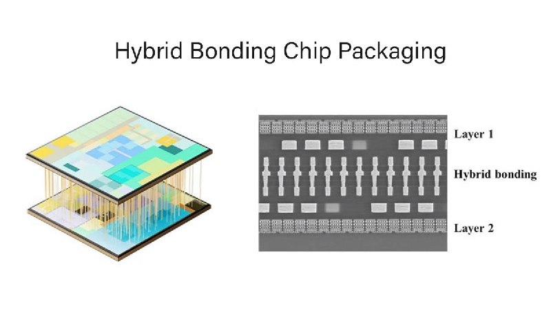
One of the most highlighted innovations within this paper is the introduction of the "hybrid bonding" process. This approach integrates disparate materials to optimize performance without the need for excessive technological dependencies.
- Efficiency: Hybrid bonding is expected to significantly improve the operational efficiency of the Kirin 2026 chipset, enabling better power consumption during tasks.
- Bandwidth: The new design concept suggests enhanced bandwidth, which is crucial for mobile devices that require high-speed data processing and transmission.
Implications for Future Huawei Mobile Processors
The findings from the Tau Scaling Law V2 paper are not mere theoretical constructs; they signify practical applications that promise to reshape the future of Huawei's mobile processing power. By leveraging hybrid bonding, Huawei aims to deliver processors that not only meet but exceed current industry standards.
| Feature | Kirin 2026 | Kirin 9000 (Previous Generation) |
|---|---|---|
| Efficiency | Enhanced through hybrid bonding | Standard efficiency |
| Bandwidth | Improved bandwidth capabilities | Limited saturation at peak loads |
| Fabrication Equipment Dependency | Minimal dependency on advanced equipment | Heavy reliance on cutting-edge tools |
Conclusion
The publication of the Tau Scaling Law V2 marks a critical step for Huawei as it navigates the complexities of modern semiconductor manufacturing. By focusing on hybrid bonding and innovative practices, Huawei is setting the stage for the Kirin 2026 chipset to rise above its predecessors, potentially transforming user experiences in mobile technology. With these advancements, Huawei reaffirms its commitment to remain at the forefront of the competitive chip market.
Huawei Tau Scaling Law V2 paper discusses many aspects that will help the firm develop the Kirin 2026 chipset without using advanced equipment, one such being the "hybrid bonding" process. The new design concept hints at better efficiency and bandwidth for upcoming Huawei mobile processors. https://www.huaweicentral.com/huawei-hybrid-bonding-for-kirin-2026-chipset/ Huawei Tau Scaling Law V2 paper discusses many aspects that will help the firm develop the Kirin 2026 chipset without using advanced equipment, one such being the "hybrid bonding" process. The new design concept hints at better efficiency and bandwidth for upcoming Huawei mobile processors. https://www.huaweicentral.com/huawei-hybrid-bonding-for-kirin-2026-chipset/


